
Semiconductor technology has been at the forefront of innovation, driving advancements in various industries such as electronics, telecommunications, and renewable energy. One crucial aspect of semiconductor manufacturing is the use of patterned wafers, which have become increasingly significant in unlocking new possibilities in this field. In this blog post, we will delve into the world of patterned wafers, exploring their fabrication process, benefits, applications, and the challenges they present. We will also discuss recent advances in patterning techniques and their impact on semiconductor technology, as well as prospects and emerging trends in this exciting field.
Source: wevolver.com
Introduction to Patterned Wafers and their Significance in Semiconductors
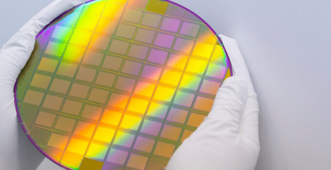
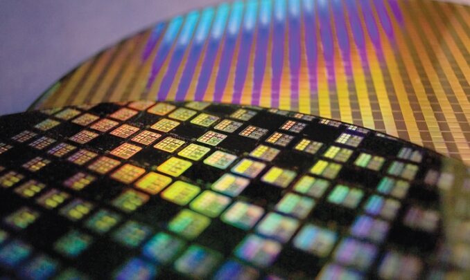
Patterned wafers, also known as shaped substrates, are semiconductor wafers with specific patterns or structures etched onto their surfaces. These patterns serve as templates for the subsequent deposition of semiconductor materials, enabling the creation of intricate electronic devices. By using patterned wafers, manufacturers can achieve precise control over the shape, size, and arrangement of electronic components on a chip. This level of control is crucial for the performance and functionality of semiconductor devices.
Evolution of semiconductor technology and the Role of patterned wafers
The semiconductor industry has witnessed remarkable progress over the years, with Moore’s Law driving continuous improvements in chip performance and density. Patterned wafers have played a pivotal role in this evolution. Initially, semiconductor manufacturing relied on simple planar wafers, but as the demand for smaller, faster, and more complex devices grew, the need for them became apparent. By introducing patterns and structures at the nanoscale, manufacturers could enhance device performance and integrate more functionality onto a single chip.
Exploring the fabrication process of patterned wafers
Source: semiengineering.com
The fabrication process involves several intricate steps. Initially, a pristine wafer is coated with a layer of photoresist, a light-sensitive material. The semiconductor is then exposed to a mask that allows light to pass through specific areas. This exposure causes a chemical reaction in the photoresist, rendering it either soluble or insoluble. Subsequent treatments remove the soluble or insoluble regions, leaving behind the desired pattern on the wafer’s surface. This pattern serves as a template for subsequent deposition processes, where these materials are added to create electronic components.
Key benefits of patterned wafers in semiconductor manufacturing
They offer numerous benefits in semiconductor manufacturing. Firstly, they enable precise control over device dimensions and characteristics, leading to improved performance and functionality. Secondly, patterned wafers allow for the integration of multiple components on a single chip, leading to increased chip density and reduced production costs. Additionally, they facilitate the development of complex architectures, such as three-dimensional integrated circuits (3D-ICs), which further enhance device performance and energy efficiency.
Applications and potential uses of patterned wafers in different industries
Shaped semiconductors offer a wide range of applications in a variety of industries. They enable the development of smaller, more powerful consumer electronics, including smartphones and wearable devices, in the electronics industry. Textured transistors aid in the creation of high-speed, wide-bandwidth communication equipment in telecommunications. Furthermore, they are used in renewable energy, allowing for the fabrication of more efficient solar cells and energy storage devices. Patterned slabs are also useful in the medical industry since they enable the construction of tiny diagnostic and therapeutic devices.
Advances in patterning techniques and their impact on semiconductor technology
Source: tomshardware.com
Significant advancements in patterning techniques have had a profound impact on semiconductor technology. Traditional optical lithography, which uses light to transfer patterns onto semiconductors, has reached its limits due to the diffraction of light at smaller feature sizes. To overcome this challenge, techniques such as extreme ultraviolet (EUV) lithography and electron beam lithography have emerged. These techniques utilize shorter wavelengths or focused electron beams, enabling the creation of finer and more intricate patterns. These advancements have paved the way for further miniaturization and increased functionality in semiconductor devices.
Challenges and limitations in the semiconductor industry
While they offer immense potential, they also present certain challenges and limitations. One major challenge is the cost associated with the fabrication process, as it requires specialized equipment and materials. Additionally, achieving uniformity and defect-free patterns at smaller feature sizes becomes increasingly difficult. Moreover, as patterns become more intricate, the potential for manufacturing defects and yield losses also increases. Overcoming these challenges requires ongoing research and development in process optimization and defect reduction techniques.
Case studies highlighting the successful implementation of patterned wafers
Several case studies demonstrate the successful implementation in various applications. For example, in the field of microprocessors, their use has enabled the continuous improvement of chip performance and power efficiency. In the solar energy sector, they have contributed to the development of highly efficient solar cells, boosting the adoption of renewable energy. These case studies highlight the transformative impact that patterned slabs can have when integrated into semiconductor manufacturing processes.
Future Prospects and emerging trends in patterned wafer technology
Source: eetasia.com
The future of this technology looks promising, with ongoing research focused on overcoming existing limitations and exploring new possibilities. Advancements in nanotechnology, materials science, and innovative patterning techniques hold the potential to revolutionize its manufacturing. Moreover, the integration with other emerging technologies such as artificial intelligence, the Internet of Things, and quantum computing could unlock entirely new applications and drive further innovation in various industries.
Potential disruptions and innovations are driven in the semiconductor sector
They have the potential to drive revolutionary developments in this industry. The ability to manufacture highly complex and small electronic devices opens the door to improvements in fields such as artificial intelligence, self-driving cars, and augmented reality. Shaped circuits have the potential to completely transform the healthcare business by enabling the development of implanted medical devices, tailored medicine, and improved diagnostic tools. Furthermore, they may contribute to the achievement of quantum computing by providing unparalleled computational capacity and addressing challenging issues that traditional computers cannot solve.
Conclusion: The transformative power in semiconductor technology
Patterned wafers have emerged as a key enabler of innovation in semiconductor technology. They offer precise control, improved performance, and increased functionality in the production of electronic devices. With advancements in patterning techniques and ongoing research, the potential applications of patterned wafers continue to expand across industries. While challenges and limitations persist, the transformative power of patterned wafers cannot be overlooked. As we look toward the future, patterned wafers hold the promise of unlocking new possibilities and driving disruptive innovations that will shape the world of semiconductor technology.


